
Vision
We are fabricating new functional devices and exploring new physics and their application positively utilizing silicon nanometer size structures or organic molecules and bio-materials. Also, we are developing both the top down and bottom up fabrication processes to fabricate these nanometer size structures.
Subject of Research
New functional silicon nanodevices
Now, the channel length of MOS transistors in LSI becomes smaller than 100nm utilizing advanced lithography techniques. We are now developing new functional devices having smaller structures such as Si nanowires with channel width of a few tens of nm or Si quantum dots by using electron beam lithography technique. We investigate new phenomena and study the physics and their applications.
Molecualr and bio devices
Organic molecular devices with lightness, flexibility and freedom from environmental pollution are key devices for the ubiquitous network society. We are developing new functional devices merging organic molecular or bio materials and LSI fabricating techniques to contribute the ubiquitous network society.
Nanodevice fabrication process
Both the top down and bottom up processes are investigated. We are developing not only the electron lithography technique for the fabrication of nanometer size structures such as quantum dots but also self organizing molecular process such as atomic layer deposition of gate dielectrics for advanced MOS transistors.
Message to prospective students
Let us enjoy fabricating new functional devices and finding new physics. In our laboratory, students acquire all-round basic knowledge of unit and total device fabrication techniques as well as device measurement techniques. After your serious study, you can research in the nanodevice and new functional device field at the front.
 |
 |
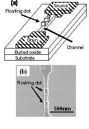 |
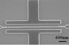
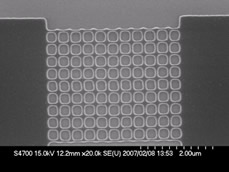
| Fig. 1. Room temperature operating silicon single electron logic (XOR) circuit with 1-dimensional regular array of silicon quantum dots. | Fig. 2. New functional device with 2-dimensional regular array of silicon quantum dots. | Fig. 3. Flash memory with silicon nanometer size floating dots. Schematic view (a) and SEM micrograph (b). |