| HIGASHI, Seiichiro Professor |
Graduate School of Advanced Sciences of Matter Department of Semiconductor Electronics and Integration Science Semiconductor Electronics |
|
Home Page : http://www.semicon.hiroshima-u.ac.jp/ | |
Vision
“First in the World, From Hiroshima” is our motto. Our study covers thin-film materials, processing, and device fabrication. We are presenting our latest results all over the world. The research subject is to contribute to the revolution of next generation electronics such as ULSI, flat panel displays, and solar cells
Subject of Research
Millisecond Annealing Induced by Atmospheric Pressure Thermal Plasma Jet and Its Application to Device Fabrication
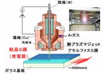
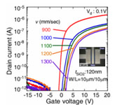
We proposed the application of DC arc discharge thermal plasma jet to millisecond annealing of semiconductor and insulator films for the first time in the world. This technique can be applied to the crystallization of amorphous silicon films on glass (Fig. 1), and we have successfully fabricated high performance thin-film transistors (TFTs) with a field effect mobility of ~350 cm2V-1s-1 (Fig. 2).
Noncontact Temperature Measurement Technique with Millisecond Resolution using A Probe Laser
We have developed a noncontact measurement technique of substrate temperature during device fabrication processing using a probe laser for the first time in the world. The temperature distribution and time evolution of surface temperature of quartz and silicon wafer is obtained (Fig. 3). This monitoring technique is quite useful to investigate crystallization mechanism and dopant activation in millisecond time domain.
Development of Silicon Microliquid Processing
We are developing a novel crystallization technique using a very small droplet of molten silicon. Generation of microliquid, crystalline growth, simulation of heat diffusion and solidification, and solar cell fabrication are under investigation.
 |
 |
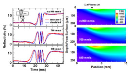 |
| Fig. 1.Crystallzation of a-Si films by atmospheric pressure TPJ. | Fig. 2.Id-Vg characteristics of TFTs fabricated by TPJ. | Fig. 3. Transient reflectivity and measured temperature distribution in quartz. |
Research Environment
Students can conduct their work in well equipped environment for semiconductor research as listed; clean room (class 1000), plasma CVD, multi-chamber CVD, photolithography, wet booth, plasma jet generator, furnace, vacuum evapolation, Raman scattering, FTIR, AFM, XPS, etc
Message to prospective students
All students in this laboratory do experiments on film deposition, characterization and device fabrication by themselves. They learn the difficulties and fun of research through the experience. The students are the driving force of this laboratory in all activities including international conferences, school events, laboratory camp and parties, etc